
In manufacturing of semiconductors, panels, boards, and other surfaces, thickness control is vital to the final product’s quality. Often, incoming substrate materials need to be measured for uniform thickness. Other times, as layers are added or bonded to surfaces the thickness needs to be constantly monitored. The best way to accurately measure thickness is by using opposing sensors to instantaneously measure both sides of the surface at the same time. This method of measurement is called Total Thickness Variation (TTV).
What Problem Does TTV Solve?
Measuring thickness with precision is challenging without the ability to measure from both sides. Even small flatness or warpage errors on a surface are hidden if only measuring from one side. In the case where a sensor is only measuring from the top side, the bottom surface’s flatness errors are hidden. This is true even if the substrate being measured is placed on a perfectly flat surface.
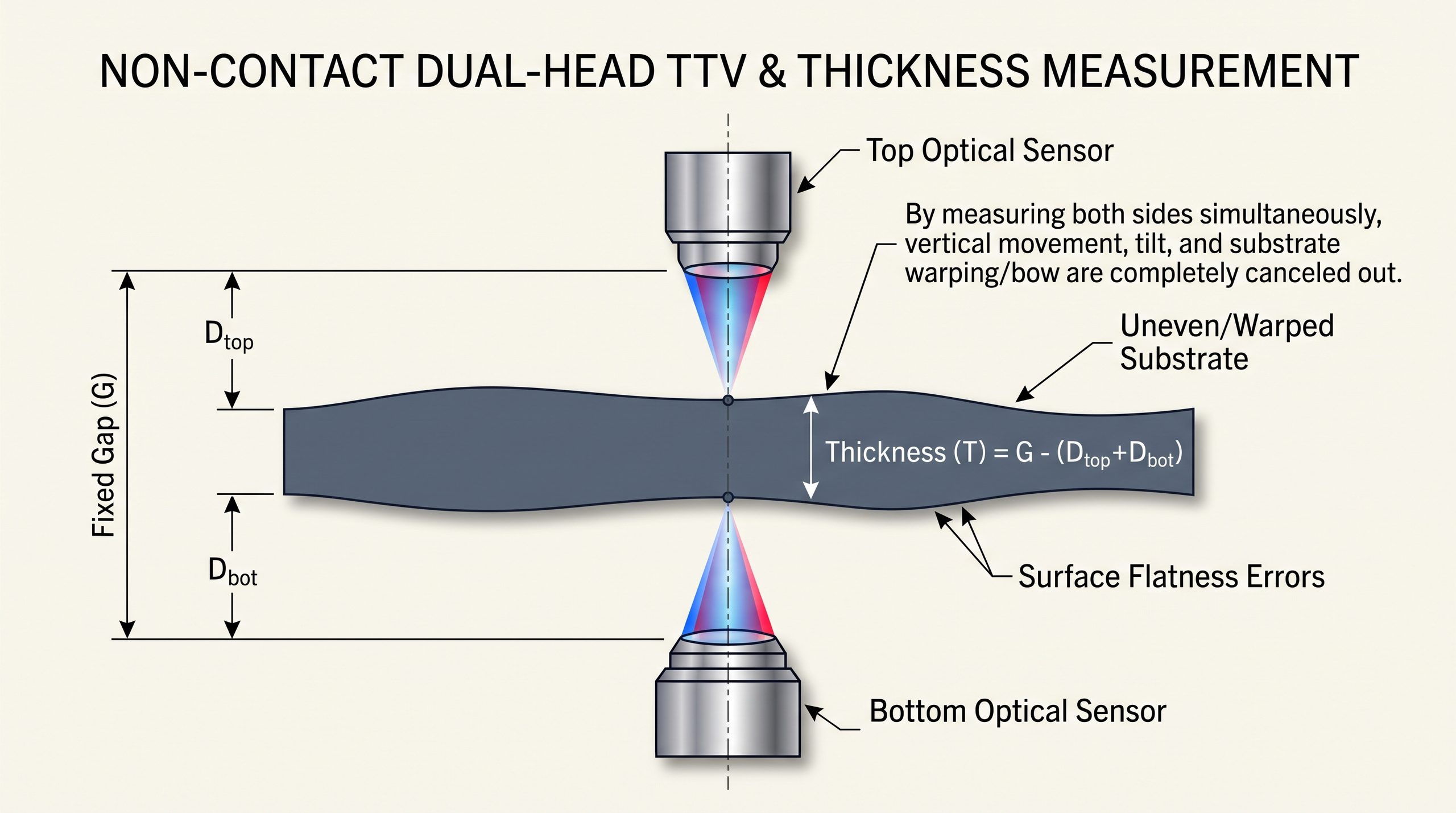
Showing opposing sensors. The surface varies on both sides, but because the sensors are measuring both sides at the same location the true thickness of the surface is recorded.
Benefits of a Dual Sided Measurement
- True Thickness Variation (TTV): Surface flatness/warpage errors on either side of the substrate are measured and included in the thickness measurement.
- Bottom and Top Surface Data: Beyond a thickness value, topography data for the top and bottom surfaces are returned individually.
- Non-Contact Measurement: Non-contact sensors can be easily aligned to point at the same location in space. This enables inspection without touching and potentially damaging the sample’s surface.
- Broad Range of Measurement: The sensors are selectable with different measurement ranges which allows for parts of different thicknesses to be measured without changeover.
- Material Agnostic: Chromatic confocal sensors are capable of quality measurement of almost any surface material.
How Accurately Can Thickness be measured?
The non-contact sensors that Peak typically incorporates are sub-micron accurate in nature. Paired with a precision PlanarDLA stage from Aerotech, we are able to keep the total measurement errors to a few micrometers or less.
System Measurement Performance
| Measurement | Specification | Notes |
|---|---|---|
| Single Sensor Linearity | +/- 0.35 µm (micrometer) | Based on a Keyence CL-S015 chromatic confocal sensor. |
| Thickness Measurement Accuracy (localized) | +/- 0.75 µm (micrometer) | Includes uncertainty from each sensor and calibration standards. |
| Fixed-Height Thickness Measurement Accuracy (over 250×250 measurement area) | +/- 3.0 µm (micrometer) | Includes additional uncertainty from stage flatness. |
| Total Thickness Measurement Accuracy (over 250x250x75 mm measurement volume) | +/- 9.0 µm (micrometer) | Includes additional uncertainty from Z-axis accuracy. |
proving out the performance with a gage R&R
Gage R&R (Repeatability and Reproducibility) tells us how much variation comes from operating the measurement tool. We put this tool to the test to understand what real measurement variation would look like under multi-part and multi-operator use. As you can see from the table below, we were able to run this tool and maintain a <2 micrometer error across various samples and operators.
Conditions of the test:
- 2 Operators
- Each measuring 8 separate 100mm wafers
- Each wafer was measured 3 separate times
- Thickness was collected at 9 different points on each wafer
- A total of 432 measurement locations
| Measurement Metric | Measurement Result | Practical Meaning |
| Total Measurement System Error | 1.61 microns | Total system variation across all equipment and operators. |
| Equipment (Hardware) Error | 0.93 microns | The optical sensor repeatedly measures the exact same spot with sub-micron precision. |
| Operator Error | 1.31 microns | Different operators obtain nearly identical thickness values across all wafers. |
Based on the thickness of the wafers measured, the above results of the Gage R&R measured at 0.60% variation.
Machine Examples
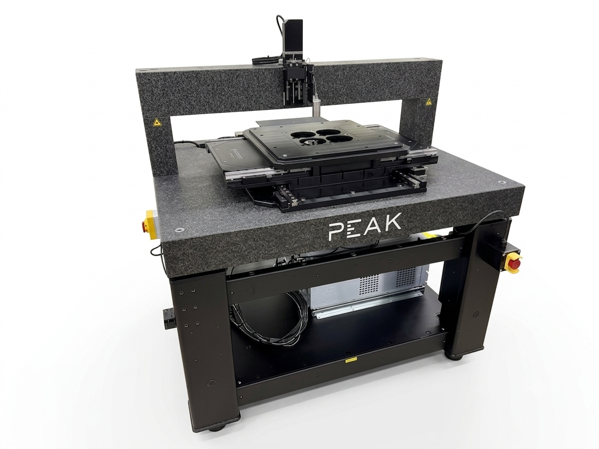

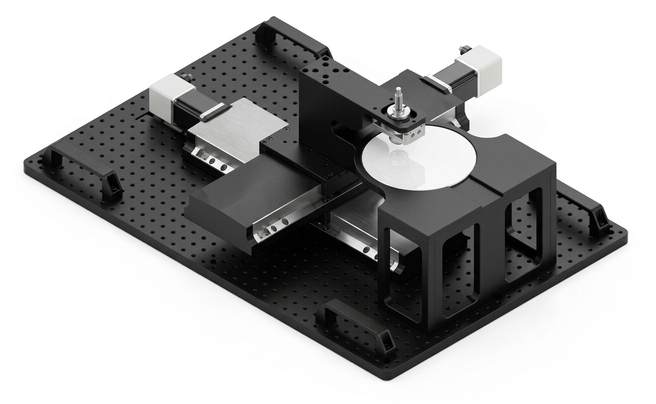
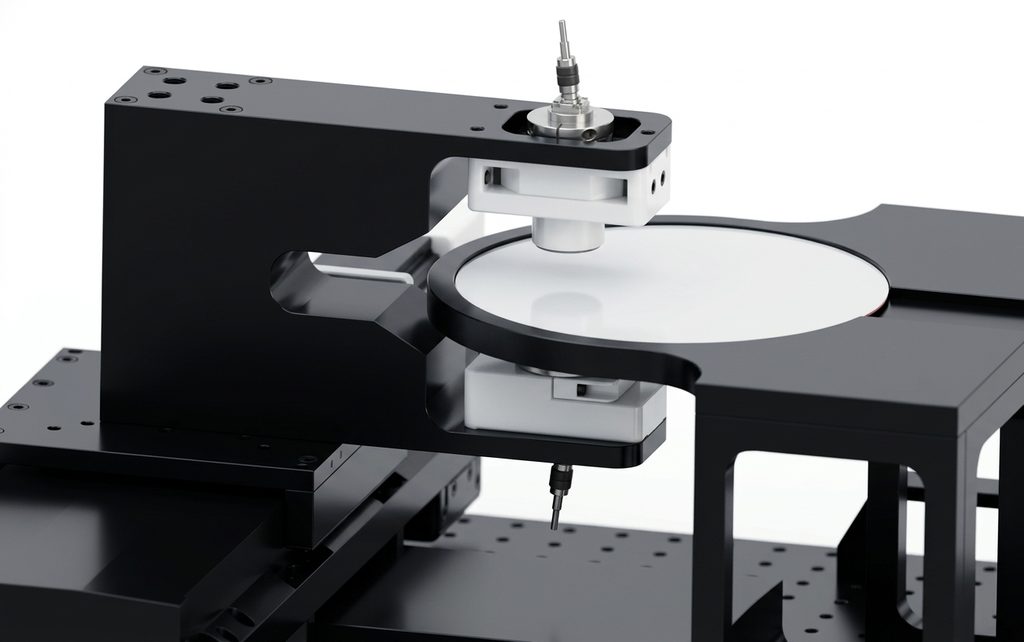
See It In Action – Video
conclusion
Relying on manual contact gauges or unguided single-sided optical tools for wafer thickness measurement introduces unacceptable yields risks, high labor costs, and measurement errors caused by wafer warpage and stage vibration. By adopting dual-head non-contact optical confocal metrology with integrated vision guidance, manufacturers can safely automate thickness profiling across all stages of substrate manufacturing.
Reach out to us for consultation so that we can guide the selection process. For more information about our measurement systems, visit our sensor integration product page.